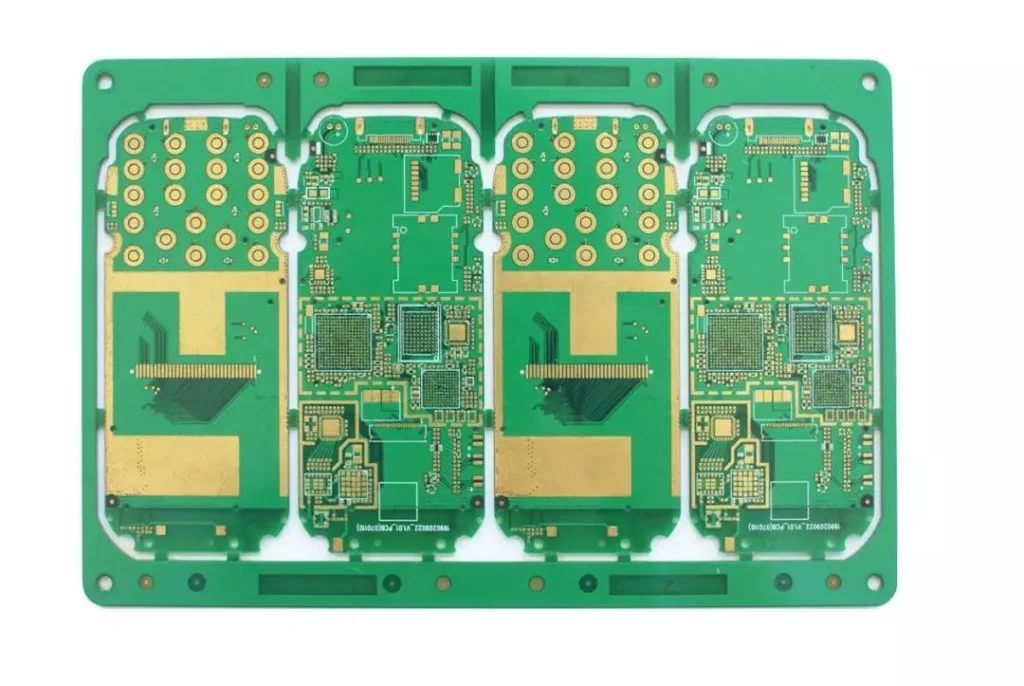
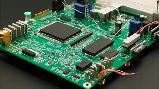
Printed Circuit Board (PCB) layout design is important in the current era of electronics because it constitutes the heart of smartphones, medical devices, and industrial control equipment. Designing is required so that electronic parts such as capacitors, resistors, and integrated circuits can be placed on a board safely and properly wired with copper lines. Excellent PCB layout is paramount to optimal performance, signal integrity, and thermal design, all of which have direct effects on electronic product performance and reliability.

PCB Layout Design: An Overview
PCB layout design is the conversion of a schematic diagram into a physical components layout and electrical connection on a printed circuit board. It is done by mounting electronic components, i.e., resistors, capacitors, and chips, in specific positions and interconnecting them with copper traces. An effective PCB layout achieves the optimum utilization of design efficiency and keeps interference at bay while making the system thermal stable.
What is a PCB?
A Printed Circuit Board (PCB) is a substrate for electronic component mounting with interconnections. It is usually composed of a mounting base material, interconnection copper layers, and insulating layers to prevent short circuits. PCBs are of various types such as rigid, flexible, and metal-core types with the latter being used for specific applications.
Key Components and Terminology
It is crucial to have knowledge of terms and components of a PCB in order to succeed in a design. A schematic diagram is symbolic representation of the circuit and also shows the connectivity of the components to one another. Surface-mount devices (SMD) are components mounted onto the surface of the PCB, whereas through-hole components possess leads that pass through the PCB. Copper traces are pieces of copper used to establish electrical connections among these components.
The PCB Design Process: Step by Step
A process from PCB to functional PCB is made up of a series of key steps:
Defining Requirements and Specifications
First of all, specifications for the requirements of the circuit in terms of voltage, current, signal stability, and temperature requirements must be defined. These clearly defined specifications then come into action to guide the process of the design and keep all constraints strictly.
Schematic Capture
By utilizing the PCB design tool, the schematic diagram is schematically drawn to signify the electrical connection of devices. It is the overall design plan of the physical PCB board.
Component Placement
Once the schematic is completed, components are installed on the PCB. Installation must consider the closeness of devices, power distribution, handling heat, and general signal route.
Routing Traces
Copper traces are made to connect the elements, which then serve as paths for the electricity. Signal integrity, power and ground planes, and proper utilization of vias are of utmost priority in this context.
Design for Manufacturability (DFM)
In this scenario, this design is optimized for production by keeping trace width, via sizes, and gap at industry standard. It’s cost-effective while producing and preserves any production defects in the future.
Production File Generation
Production files like Gerber files and a Bill of Materials (BOM) are generated. They incorporate data used to manufacture the PCB.
Testing and Verification
The design rule check (DRC) is performed with caution to check the layout prior to production. This confirms that the design according to all the electrical as well as the manufacturing requirements.
PCB Layout Tips for Best Performance
It involves some considerations that must be achieved in order to achieve the optimal performance in a PCB layout:
Noise Reduction
Noise is an important aspect of the PCB performance, especially in sensitive electronic circuits. Minimize noise by placing grounding capacitors near power pins, minimize data lines, and separate digital and analog signals.
Thermal Management
Appropriate thermal management is required in preventing component overheat. Copper pours, thermal vias, and ensuring sufficient spacing of heat-emitting components are some of the methods utilized in effective heat dissipation.
Power Integrity
In ensuring safe power, use solid power planes and ground and create wide power traces to reduce voltage drop and resistance.
Controlling Trace Length
Employ traces with the shortest possible lengths to reduce the chances of signal interference. Traces that are long are antennas that radiate unwanted radiation and can interfere with other equipment.
Use of Right Angles
Right and acute angles of PCB design must be avoided since they result in unwanted radiation and poor signal integrity. Use of rounded corners improves process performance and reduces interference.
Avoiding Common PCB Design Errors
Even an experienced PCB designer can make mistakes. Some of the usual mistakes are:
Ignoring Component Datasheets
Component datasheets have crucial information regarding component placement as well as routing specifications. Without these documents, components can be misplaced as well as cause circuit failure.
Insufficient Spacing
Spacing is performed to prevent short circuits and arcing between the components. Even the high-voltage components, in practice, need proper spacing so that there will be no electrical hazard.
Incorrect Application of Vias
Redundant or doubled-up vias may lead to signal degradation and extra resistance, impairing PCB performance.
Exclusion of Design Rule Checks (DRC)
Skipped DRCs may result in layouts that are in violation of manufacturing rules, leading to costly error during manufacturing.
Applications of PCB Design in Industry
PCB design plays a vital role in industries where functionality and reliability are involved:
Aerospace Systems
In space exploration, PCBs are utilized in mission-critical systems including navigation, communications, and control of aircraft where multi-layer and high-density PCB designs are a must.
Renewable Energy Solutions
PCBs are significant in renewable energy solutions like solar inverters and wind turbines, where they enable efficient energy control and conversion.
Smart Home Automation
PCBs facilitate seamless integration in smart home solutions like lighting, security cameras, and controllers for home automation.
Robotics and Automation
PCBs are utilized in motor control, sensor integration, and communication in robot and automation networks.
Environmental Monitoring Systems
PCBs are employed in environmental monitoring devices such as temperature, humidity, and air sensors where the major objective is wireless data transmission combined with power reduction.
Selecting the Correct PCB Components
Selecting the correct components is crucial to sustaining PCB performance and reliability. Consider:
Component Specifications
Components possess specific voltage, current, and tolerance requirements that need to be met in order to enable them to function optimally within the circuit.
Environmental Factors
Components need to be able to tolerate temperature ranges, humidity, and other environmental conditions relevant to the device application.
Component Availability
Select those components which are readily available and low-cost but high on reliability and quality.
PCB Routing Techniques in Detail

Optimal routing is an art of striking a balance between signal integrity, manufacturability, and area utilization. Some of the key techniques to be followed are:
Trace Width and Spacing
Traces with wider widths need to be used for larger currents, and adequate trace spacing between them prevents signal interference and maintains the PCB design standard.
Differential Pair Routing
For differential pairs of high-speed signals, routing should be done in a controlled impedance to maintain signal integrity and prevent reflection.
Via Usage
Overuse of vias can degrade signal quality, and therefore should be minimized while layer connectivity is ensured.
Power and Ground Planes
Power and ground planes maintain voltage at stable levels and noise at minimum levels to provide dependable circuit performance even at high frequencies.
Minimizing Dangling Lines
Dangling lines should be prevented since they act as antennas and introduce radiation interference.
Self-loop Routing
Self-loop routing should be prevented since it introduces radiation interference, which adversely affects the performance of the PCB.
Ground Loop Minimization
Reducing the area of the loop formed by a signal trace and the return path reduces ground loops and overall stability of the circuit increases.
Power Distribution Network (PDN)
There needs to be a well-designed Power Distribution Network (PDN) to provide stable and efficient power to all the components on the PCB. The key components of the PDN are:
Power Planes
Power planes distribute voltage on the PCB to an even supply to all the components.
Decoupling Capacitors
Noise is filtered and voltage stabilized by these capacitors in order to have error-free operation.
Voltage Regulators
Voltage regulators provide constant voltage levels, thereby no power fluctuations happen to disrupt component operation.
Power Traces
Power traces supply power to the rest of the components on the PCB so that all components get power they need.
PCB Design for Manufacturability (DFM)
Design for manufacturability makes sure that the PCB can be produced at an economic cost, effectively, and to industry standards. Some of them are:
Design Rules
Adhering to the design rules makes sure the PCB is fit for mass production and is up to all manufacturing standards which are applicable.
Component Placement
Parts need to be positioned so they are convenient to assemble, keeping production time and cost low.
Trace Width and Spacing
Production within design specifications keeps trace spacings and widths to the required specification for intended operation.
Testing and Inspection
The design needs to be easy to test and inspect in order to preserve quality and performance levels during manufacturing.
PCB Design and Production with Silkbridge

For premium pcb design and manufacturing, Silkbridge is a top electronic manufacturing and service solutions company. Its mission of British innovation combined with Chinese efficiency in manufacturing guarantees high-quality PCBs manufactured according to diverse requirements. Offering a complete range of services that also encompasses plastic injection molding, electronic product assembly, and PCB product and design, Silkbridge is a one-stop-shop to turn your electronic designs into reality.
To learn more about the pcb design and manufacturing available from Silkbridge, reach out to their team at contact@silkbridgeltd.com. Or their whatsapp link https://wa.me/8618122838771


