Why PCB Design for Manufacturing (DFM) Reviews Are Critical
The Cost of Overlooking DFM Principles
A PCB design that appears flawless on a screen might still falter during production if Design for Manufacturing (DFM) principles are ignored. Without a careful evaluation, problems such as overly narrow traces, improperly aligned solder masks, or cramped component layouts can trigger expensive fixes. Correcting a defective PCB design raises production expenses significantly. It also postpones the product’s release. In large-scale manufacturing, even a tiny flaw can produce thousands of faulty units. This leads to substantial monetary losses and harms the company’s reputation.

Common Manufacturing Errors Linked to Poor Design
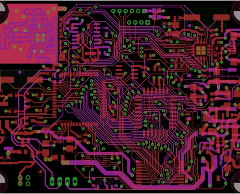
Numerous PCB manufacturing mistakes stem from basic oversights in planning. Inadequate spacing between traces can cause short circuits or interruptions, particularly in fast-signal designs. Undersized pads might weaken solder joints, resulting in assembly breakdowns. Uneven copper distribution may warp the board during creation, compromising its strength. Furthermore, poorly positioned drill holes can complicate production and inflate costs. These issues emphasize the need for a detailed DFM review to spot errors before production starts.
How DFM Impacts Time-to-Market and Product Reliability
A thorough DFM review accelerates product creation by avoiding surprises during fabrication and assembly. When a design is tailored for manufacturing, it transitions smoothly from testing to full-scale output. This shortens delivery timelines and stabilizes the supply chain. Additionally, a carefully inspected design boosts product dependability, lowering the chances of failures after deployment. Firms that emphasize DFM often enjoy greater customer approval and a stronger market position.
Key Steps to Review PCB Designs for Manufacturing Errors

Start with a PCB Design for Manufacturing Checklist
A well-organized checklist guarantees that no vital element of the PCB design is missed. Begin by confirming the layer arrangement and material choices suit the intended purpose. Next, verify that trace widths and gaps match the manufacturer’s limits to avoid signal problems or shorts. Ensure components have ample room around them. Also, check that via placements follow fabrication rules to prevent stress on the board. Addressing these aspects early saves both time and money later.
Apply PCB Design for Manufacturing Guidelines
Sticking to proven PCB design for manufacturing guidelines ensures a trouble-free shift from concept to creation. Component positioning is vital, especially for automated assembly systems. Misplacement can cause soldering errors, raising defect numbers. Heat control matters too—insufficient cooling can damage parts. Copper distribution should be even to avoid bending and ensure uniform plating during production. Following these standards improves the PCB’s manufacturability.
Address Commercial Application-Specific Requirements
Various sectors demand distinct features from PCB designs. In industrial and healthcare settings, managing electromagnetic interference (EMI) and compatibility (EMC) is crucial to avoid signal issues. Automotive PCBs need tough designs to endure heat and shaking. For commercial applications, designers must focus on power savings, size reduction, and eco-friendly rules. Tailoring the PCB design to specific industry needs secures approval and lasting performance.
Advanced Strategies for Error-Free PCB Manufacturing
Leverage AI-Driven Design Analysis Tools
Artificial intelligence is transforming PCB design with smart error prediction. AI tools can detect potential solder mask misplacements, preventing production flaws. They also mimic heat and physical strain, helping designers refine material and layout choices. Automated checks speed up reviews and boost precision, lessening the need for manual oversight. By embedding AI in the workflow, engineers catch mistakes early and enhance production efficiency.
Collaborate Early with Your Manufacturing Partner
Teaming up with the PCB manufacturer from the start aligns design goals with production abilities. Sharing files early lets manufacturers spot issues like tricky via setups or unsuitable finishes. Matching their tolerances and limits lowers the odds of late tweaks that slow things down. This teamwork ensures the design meets both function and manufacturing needs.
Test with Functional Prototypes
Before launching full production, working prototypes test the design in real conditions. These models expose assembly flaws like tombstoning or bridging, which simulations might miss. Signal tests check if the PCB meets performance goals, especially in rapid applications. Fixing problems during prototyping cuts defect rates and ensures a solid final product.
PCB Design for Manufacturing and Assembly Best Practices

Optimize for Automated Assembly Processes
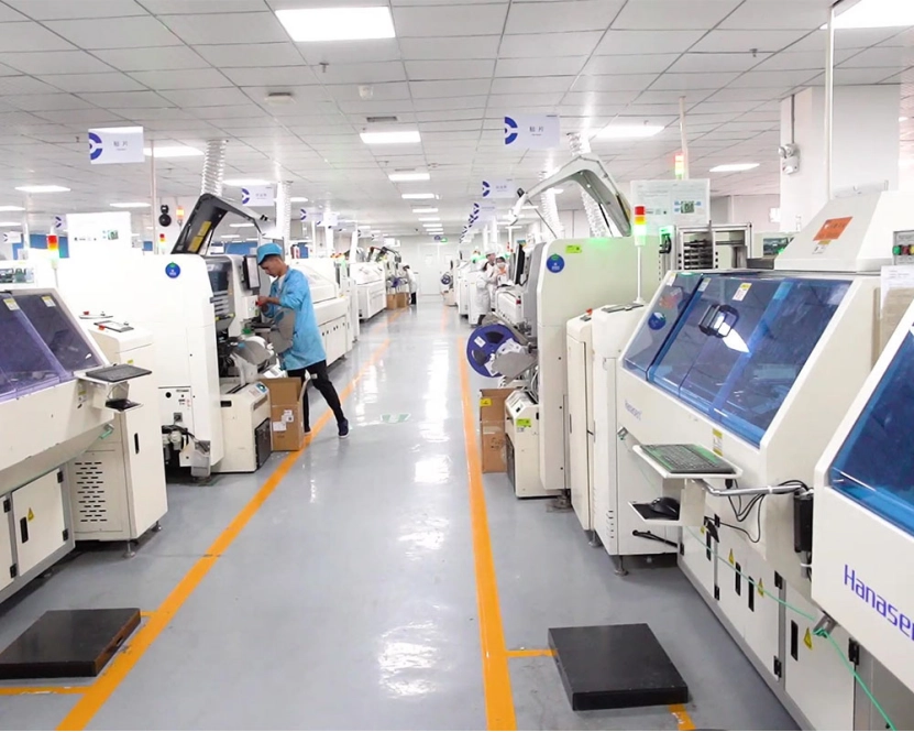
Today’s PCB assembly depends heavily on machines, and designing for pick-and-place systems boosts efficiency. Correct part alignment reduces errors and hastens assembly. Panelization plans should minimize waste and ease handling. A finely tuned design lifts success rates and trims costs.
Avoid Hidden Costs in PCB Fabrication
Some design decisions can quietly hike fabrication expenses. Via-in-pad layouts, while great for dense designs, complicate production and raise costs. Tricky drilling patterns might need special tools, pushing expenses higher. Choosing standard finishes like HASL over ENIG balances performance and affordability. Watching these details keeps costs in check.
Design for Testability and Repairability
Adding test points to the PCB layout simplifies in-circuit testing (ICT), aiding quick quality checks during assembly. Test features help pinpoint faulty units fast, improving output rates. Also, planning for repairability lets broken parts be swapped out easily, lengthening the product’s life. A smart design supports both production and upkeep.
Industry-Specific PCB Design Considerations
High-Density Interconnect (HDI) for IoT and Wearables
HDI PCBs are key for tiny devices like IoT sensors and wearables. Proper microvia placement and following blind/buried via rules ensure signal strength and durability. These designs need exact fabrication methods to perform in small sizes.
Rigid-Flex PCB Challenges in Aerospace
Aerospace often uses rigid-flex PCBs for light, space-saving designs. Yet, these must meet tough reliability rules. Setting the right bend radius prevents wear, cutting failure risks in active settings. Aerospace PCBs must also handle extreme heat and motion.
Medical-Grade PCB Requirements
Medical tools need high precision and rule compliance. Cleanroom assembly often ensures cleanliness, while safe coatings protect patients. Designing these PCBs demands strict quality steps to meet standards and avoid critical failures.
Building a Collaborative Workflow with Manufacturers
How to Interpret Gerber Files and Drill Charts
Knowing Gerber files and drill charts is vital for clear talks with PCB makers. These files detail copper layers, solder masks, and hole spots. Ensuring their accuracy avoids production mistakes and confusion.
Resolving Conflicts Between Design and Production Teams
Designers and makers sometimes see PCB production differently. Open talks and early teamwork sort out issues like part sourcing, tolerances, and methods. Regular reviews keep everyone aligned and cut last-minute fixes.
FAQs: PCB Design for Manufacturing
What’s the most overlooked item in a PCB design for manufacturing checklist?
Annular ring width for plated through-holes is often misjudged, causing fabrication hiccups.
How do commercial applications impact PCB material selection?
Fast-signal uses need low-loss materials like Rogers to keep signals clear.
Can automated tools replace manual DFM reviews?
Automated tools spot about 80% of errors, but human skill is still key for tricky designs.
Why is panelization important for PCB assembly?
Panelization cuts handling time and boosts output, especially for small boards.

Make sure your PCB designs are ready for production with Silkbridge PCB Design and Manufacturing. Silkbridge blends British innovation with Chinese manufacturing efficiency. Founded in 2014 by a British design engineer and based in Guangdong, China, we lead in high-quality manufacturing solutions.
Our skills in IoT, medical, and industrial uses ensure designs flow smoothly into manufacturing. Reach out Silkbridge today at contact@silkbridgeltd.com. Or use our WhatsApp link https://wa.me/8618122838771 with your questions for a DFM checklist or design advice.


