In the computer era, the printed circuit board (PCB) is the unsung hero of our machines. PCBs are ubiquitous all around us, from our smartphones to the machines in the factory shop floor, but not many know what they do. The following is an attempt to explain PCBs, a basic rundown of their components, categories, and designing process. Whether you are a hobbyist who wants to make your own PCB or an engineer who wants to know more, you will find something on this site that is for you both.
What is a PCB?
A printed circuit board (PCB) is a rigid material insulating flat board of insulating material, usually fiberglass (FR-4). It is a substrate upon and with which electronic components like resistors, capacitors, integrated circuits, and transistors are mounted and electrically connected. Instead of employing bulk wires for wiring parts, PCBs are made up of copper traces that are thin and lightweight on the board top. The trace is wire-like in nature and allows electrical signals to pass between parts. Aside from facilitating easier assembly of circuits, this also allows electronic devices to be made smaller so that they are efficient, light, and compact.
Composition
- Substrate: The substrate comes to reside inside the inner cavity of a PCB. It serves to give the whole board physical support. As explained earlier, FR-4 fiberglass is used as the common material for the substrate due to its improved electrical insulation characteristics, hardness, and comparatively intermediate cost. In specific situations, such as high-frequency circuits or usage that demands very high heat resistance, other constituents of the material of the substrate material, i.e., ceramics or polyimide, can be used instead.
- Copper Layers: Single or multiple copper layers along the edge of the substrate. These are where the magic happens – they carry the electricity from component to component. The single-side PCB has only one copper layer, but double-side PCBs have copper layers on both sides of the substrate. Multilayer PCBs can have any internal number of copper layers, plus the outside layers. Copper planes are commonly etched in plane, pad, and trace patterns. Traces are narrow lines between parts, pads are where the parts connect to the board via solder, and planes are huge flat copper areas, generally for power distribution (i.e., ground plane) or signal traces.
- Solder Mask: The solder mask layer appears on copper layers to guard against oxidation, corrosion, and shorts of copper trails by chance. It’s commonly green-colored (blue, red, black being common ones also), and apertures (vias) in the layer expose pads over which components would be soldered onto. Solder mask acts to disallow unwanted spaces where soldering solder would find entry when soldering to enable making solid clean contact.
- Silk Screen: Silk-screen layer is the top layer of a PCB and is used to label text, symbols, and graphics on the board. It includes component designations (i.e., R1 for resistor 1, C2 for capacitor 2), reference marks, and other debug, test, and assembly information. The silk-screen layer is white or black color inked and a visual warning to anyone assembling, testing, and debugging the PCB.
Types of Printed Circuit Boards
- Single – Sided PCBs: The single – sided PCBs consist of one copper layer, as the name indicates. One side is loaded with components and copper traces are on the other side. They are the most simple and least expensive type of PCB and utilized in extensive applications on simple consumer commodities such as bare-bone toys, commodity power supply, or other cheap consumer commodities. Since the simplest to produce, this restricts their use to very basic circuit boards.
- Double – Sided PCBs: Double – sided PCBs have copper on both the front and rear of the substrate. This offers the potential for more advanced circuit boards since components can be placed on each side and traces can link components on the opposite side of the board. Vias are drilled through the board to provide a path of connection between the two sheets of copper with one another. Double-sided PCBs are used in such widespread applications as automotive electronics, lighting from LEDs, and some mid-range consumer electronics.
- Multilayer PCBs: Multilayer PCBs are made of several layers of copper, typically interleafed by layers of insulating material (prepreg). Boards are 4 to 40 or more layers thick. Extra layers have far higher component packing density and more complex routing and are used in high-performance equipment like computer motherboards, graphics cards, and high-speed communications devices. They are more expensive to produce, however, and more difficult to repair or rework.
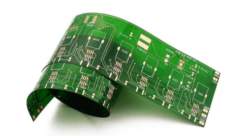
- Flexible PCBs (Flex PCBs): Flex PCBs have a bendable base material, i.e., polyester or polyimide. Therefore, they are also foldable, twistable, or bendable and hence can be used in those projects where the use of normal rigid PCBs will be inconvenient. They are used in products like smartphones, wearable devices, and interior automotive parts, where it is encapsulated to offer space while the ability to hold any shape is of topmost importance. The flex PCB can be single-sided, double-sided, or multi-layer.
- Rigid – Flex PCBs: Rigid – flex PCBs are a combination of rigid and flexible PCBs. Rigid – flex PCBs are made up of rigid and flexible components, which are laminated. This makes it possible to develop intricate three-dimensional frameworks that are able to display the mechanical stiffness of a rigid board but have the ability to bend to channel the circuits in space-constrained areas. Rigid – flex PCBs are utilized in high-end electronics, aerospace, and in medical devices.

Key Terms to Remember
- Via: A via is a plated hole drilled directly through the PCB. It is used for connecting different levels of the board so that electrical signals may be transmitted from one level to another. There are a few various types of vias, including through-hole vias (which pass entirely through the board), blind vias (which pass partially through the board and connect an outer layer to an inner layer), and buried vias (which pass entirely through the board and connect two internal layers).
- Pad: A pad is a patch of circular or square copper on the board top on which a component lead or solder joint is built. Pads are used to physically and electrically interface the components with the board.
- Trace: Trace is a thin conductive line on the PCB used to link components. Traces have a similar purpose as the wires used in a standard circuit and are used solely for the purpose of passing electric signals from component to component.
- SMT (Surface – Mount Technology): SMT stands for mounting electronic components onto the PCB without using through-hole leads. SMT components are miniature and more densely packed compared to older through-hole components, and offer higher component packaging density and smaller PCBs. It is commonly used in today’s electronics production.
- BGA (Ball Grid Array): BGA is a bottom surface mount package of an integrated circuit. In place of edge leads, packages of BGA employ a matrix of very fine solder balls in the package bottom that are attached directly to the PCB pads via soldering. It accommodates higher counts of electrical connections over a smaller region and is quite suitable for high pin count package packages.
FAQs
1. What are the differences between a single-sided and a double-sided PCB?
A single-sided PCB is made of one layer of copper, whereas a double-sided PCB is made of copper layers on opposite sides of the substrate. Double-sided PCBs allow for more complex circuit topologies and component densities.
2.Can a PCB be designed without EDA software?
While it is theoretically possible to design a simple PCB with no EDA software, it is better if more sophisticated ones are designed by utilizing the aid of EDA software. There are many EDA software features that help with designing, e.g., schematic capture, editing layout, and rule checking.
3.HOW LONG TO MAKE A PCB
PCB manufacturing time is a function of some of the parameters such as design complexity, number of layers, order size, and process. Simple design single-layer PCB might take days, whereas multilayer complex PCB might take weeks.
4.Why do PCB design errors occur?
Classic PCB problems are signal integrity problems (signal interference, signal attenuation, etc.), power delivery problems (power dissipation, voltage drop, etc.), thermal problems (device overheating, etc.), and manufacturability problems (trace width or via size, etc.).
Conclusion

Printed circuit boards (PCBs) are a basic building block of contemporary electronics which allow us to enjoy the small, high-powered devices we now all seem to take for granted. Understanding how PCBs work, their design, types, and how they are manufactured is to the benefit of any person who is an expert in the electronics world. You can be new or an expert but there is always additional knowledge on PCBs you can acquire. If you require professional PCB manufacturing services, Silkbridge has qualified experts whose service is capable of meeting your need. Don’t hesitate to reach Silkbridge at contact@silkbridgeltd.com. Or our whatsapp link https://wa.me/8618122838771 with your questions or guidance regarding your PCB design and production project – we exist to assist you in bringing your electronic concepts into reality!


