Introduction to High Density Interconnect PCB Boards
What is HDI PCB?
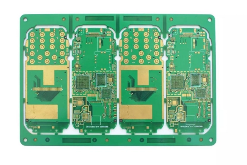
High Density Interconnect PCB, or HDI PCB, is a special type of circuit board. It packs more components into a smaller space than regular boards. This happens by using tiny wires and holes called vias. These boards help make devices like phones and cars smaller and smarter. At its core, what is HDI PCB? It’s a way to fit advanced tech into tight spaces.

The Rise of High-Density Interconnect in Modern Electronics
Years ago, electronics were big and bulky. Now, thanks to high-density interconnect HDI PCB, things have changed. Since the 1990s, companies have used these boards to shrink products. Today, they’re everywhere—think smartphones, watches, and even medical tools. The demand keeps growing because people want smaller, faster gadgets.
Overview of the High Density Interconnect PCB Market
The high density interconnect PCB market is booming. More industries need these boards for their products. Experts say this market will keep expanding as tech gets more complex. Companies like Silkbridge are part of this growth, offering high density interconnect PCB boards to meet modern needs.
Types of HDI PCBs and Their Applications
Single-Layer vs. Multi-Layer HDI PCB
HDI PCBs come in different styles. A single-layer HDI PCB has one level of wiring. It’s simple and cheap. But an HDI multilayer PCB has many layers stacked together. This type handles more power and speed, making it perfect for advanced devices. Both have their uses, depending on the project.
Applications in Smartphones, IoT, Medical, and Automotive Devices
Where do you find HDI PCBs? In smartphones, they make screens and chips fit in your pocket. For IoT, or Internet of Things, they connect smart homes. In medical devices, like heart monitors, they save lives with tiny, reliable parts. Cars use them too, especially in electric models, thanks to HDI PCB manufacturing process advancements.
Flexible and High-Frequency HDI PCB Variants
Some HDI PCBs bend, called flexible variants. Others work with fast signals, known as high-frequency types. These special boards fit unique needs. For example, a flexible HDI multilayer PCB might go into a wearable device, while high-frequency ones power 5G tech.
Key Advantages of HDI PCBs
Compact Design and Space Optimization
One big perk of HDI PCBs is their size. The advantages of HDI PCB include fitting more into less space. This means smaller devices without losing power. Designers love this for creating sleek, modern products.
Enhanced Signal Integrity in HDI Multilayer PCB
HDI multilayer PCBs keep signals clear. With tiny vias and short paths, data moves fast and clean. This matters in high-speed tech, like computers or gaming systems, where delays can ruin performance.
Improved Electrical Performance for High-Speed Applications
Speed is key in today’s world. HDI PCB design boosts electrical performance. It handles fast signals better than older boards. This makes it a top choice for things like Wi-Fi routers or car sensors.
Reliability and Durability in Demanding Environments
HDI PCBs last long, even in tough spots. Heat, vibration, or moisture won’t stop them easily. This reliability shines in cars or medical tools, where failure isn’t an option.
HDI PCB Design Fundamentals
HDI PCB Layout Best Practices
Good HDI PCB layout starts with planning. Designers keep wires short and neat. They avoid crowding parts. This helps the board work well and stay small. A smart layout is the heart of HDI PCB design.
Micro-Vias, Blind Vias, and Buried Vias Explained
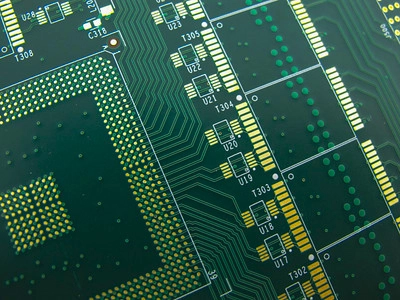
HDI boards use special holes. Micro-vias are super tiny and connect layers. Blind vias link the surface to an inner layer. Buried vias stay inside, hidden from the top. These tricks make HDI PCB layout fit more in less space.
Considerations for Fine-Pitch Components in HDI Designs
Fine-pitch parts are small and close together. Designers must be careful. They need exact measurements for HDI PCB manufacturing. This ensures every piece fits and works right.
The HDI PCB Manufacturing Process
Step-by-Step HDI PCB Manufacturing Overview
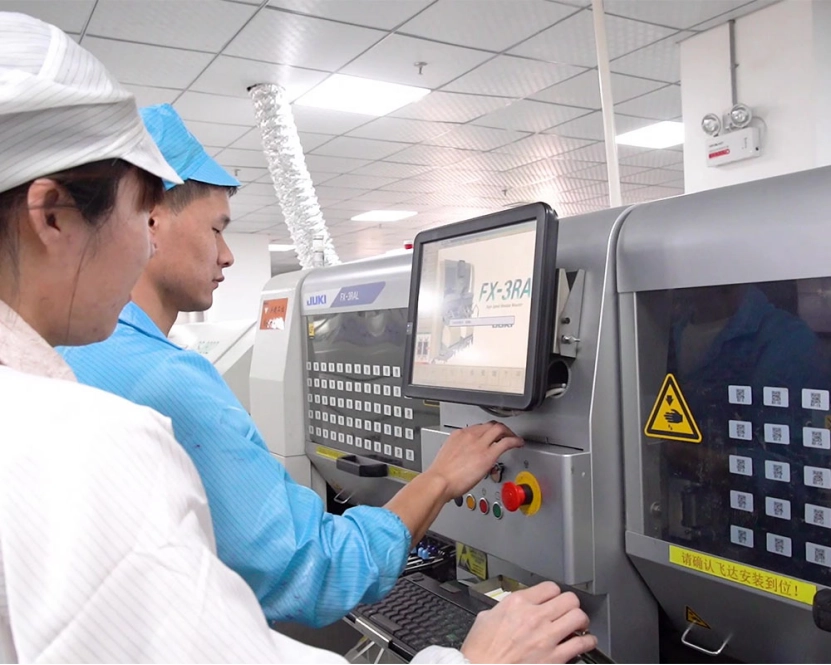
Making an HDI PCB takes steps. First, a base layer is built. Then, layers get added with wires and vias. Machines drill tiny holes and add metal. Finally, the board is tested. This HDI PCB manufacturing process creates high-quality results.
Key Materials Used in HDI Multilayer PCB Fabrication
Materials matter in HDI multilayer PCB work. Copper makes the wires. Special plastics, like FR4, form the base. Some boards use advanced stuff for heat or speed. Good materials mean better boards.
Challenges in the ProceHDI PCB Prototype Production
Building an HDI PCB prototype isn’t easy. Tiny parts can fail if not perfect. Drilling micro-vias takes skill. Costs can rise too. But solving these issues leads to great designs.
Quality Control and Inspection Standards
Every board gets checked. Machines and people look for mistakes. They test signals and strength. High standards in HDI PCB manufacturing keep products safe and reliable.
Why Choose Silkbridge High Density Interconnect PCB Boards Customization Service
Silkbridge stands out in the high density interconnect PCB market. We mix British ideas with Chinese production skills. Founded in 2014, our team in Guangdong, China, knows HDI PCB design inside out. We offer custom high density interconnect PCB boards for tough projects. Our expertise covers HDI PCB layout and manufacturing, ensuring top results.
Need a board for a phone? We’ve done it. How about car parts or medical gear? We’ve got case studies showing success. With over 100 machines, we handle big and small jobs. Our Silkbridge High Density Interconnect PCB Boards Customization Service tailors solutions to fit your needs. From start to finish, we make complex electronics simple and strong.
Getting Started with Your HDI PCB Project
How to Evaluate Your Design for HDI Compatibility
Starting an HDI project? Check your design first. Look at size and speed needs. Can it use micro-vias? Think about power too. This helps you pick the right HDI PCB design path.
Key Considerations Before Choosing an HDI Manufacturer
Pick a maker wisely. Ask about their HDI PCB manufacturing process. Do they test well? Can they handle your project size? Silkbridge offers clear answers and proven skills.
Steps to Request a HDI PCB Prototype from Silkbridge
Ready to try? Contact Silkbridge for an HDI PCB prototype. Share your design. We’ll review it and suggest tweaks. Then, we build and ship it fast. It’s that easy to start.
Ready to Power Your Project? Contact Silkbridge
Want to boost your next big idea? Silkbridge has the HDI PCB manufacturing expertise you need. Our team is ready to help with custom solutions. Call us at +86 8618122838771 or chat on WhatsApp at https://wa.me/8618122838771. Explore how our Silkbridge High Density Interconnect PCB Boards Customization Service can speed up your work. Let’s power up your project together—reach out today!


